 中文
中文


Founded in 2024, Huipu Optics is a technology company focused on the research and development of semiconductor microscopic imaging technology. The company was jointly established by Zhongke Huiyi, Wordop and Otter Optics, bringing together leading scientists, cutting-edge researchers and experienced industry experts in the field of high-speed imaging and optoelectronics, and the core members have more than 20 years of optical design and processing experience. The core components of the company's products: mirror barrel, objective lens, lighting, focusing, Z-axis and switcher are all independently developed and produced, and the whole supply chain and full stack technology are independent and controllable. Huipu Optics always regards technological innovation as the core of enterprise development, constantly explores cutting-edge technologies, and is committed to presenting customers with high-quality images with clear details and distinctive features.
Technical Innovation and Differentiation | Accurate Positioning of Market Demand | Efficiency Optimization of Whole Process
Understand customer needs deeply | Provide professional suggestions and design schemes | Provide quality after-sales service.
Strict quality management system | Continuous improvement of products | Multiple testing of products

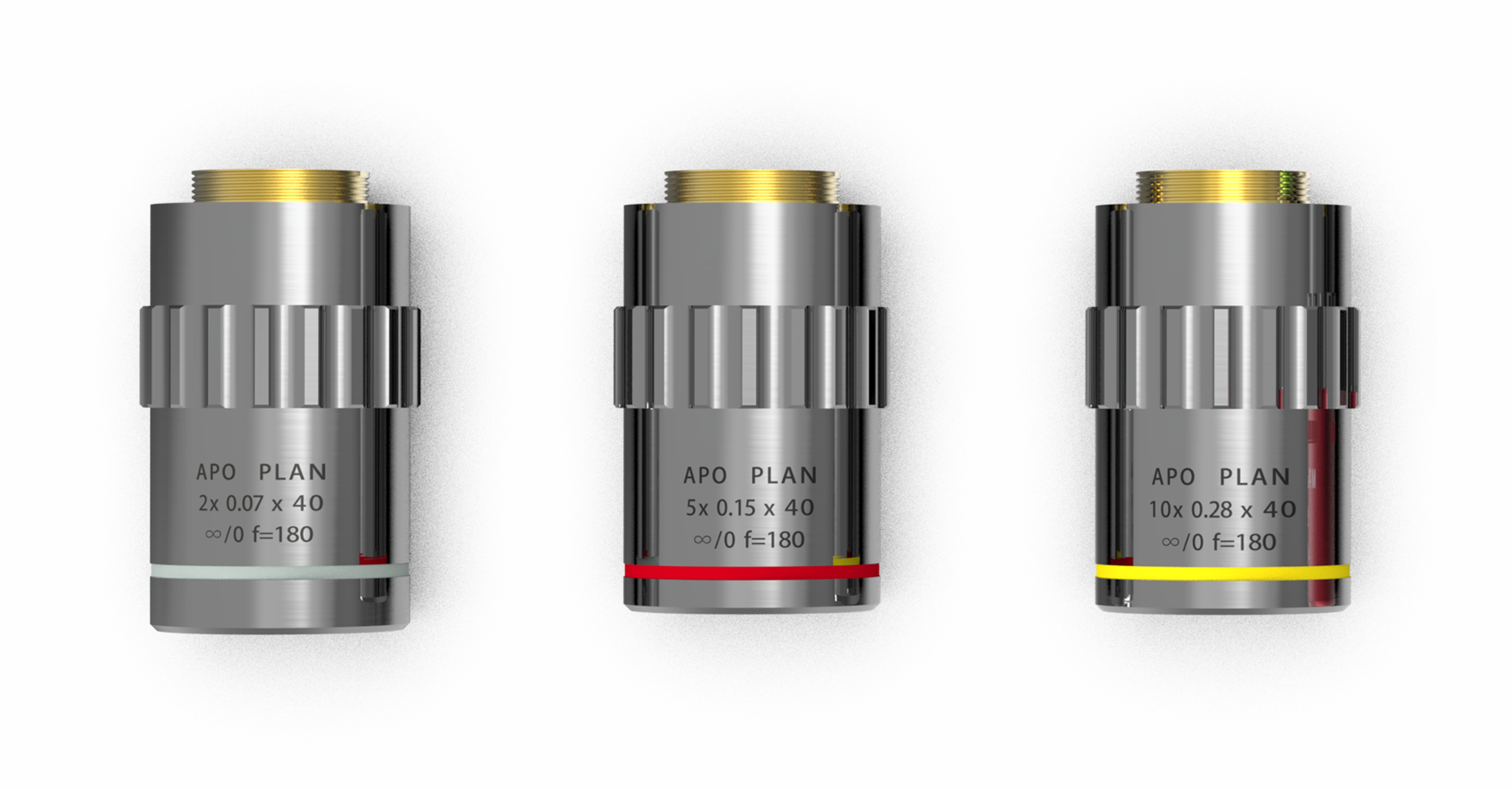
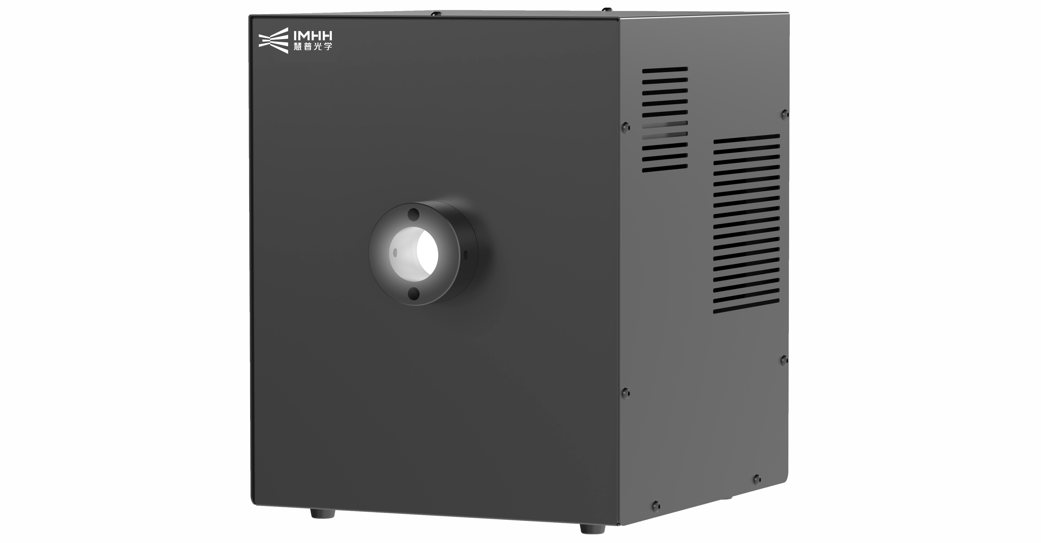
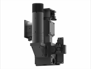
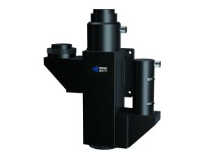
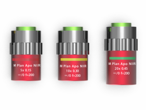
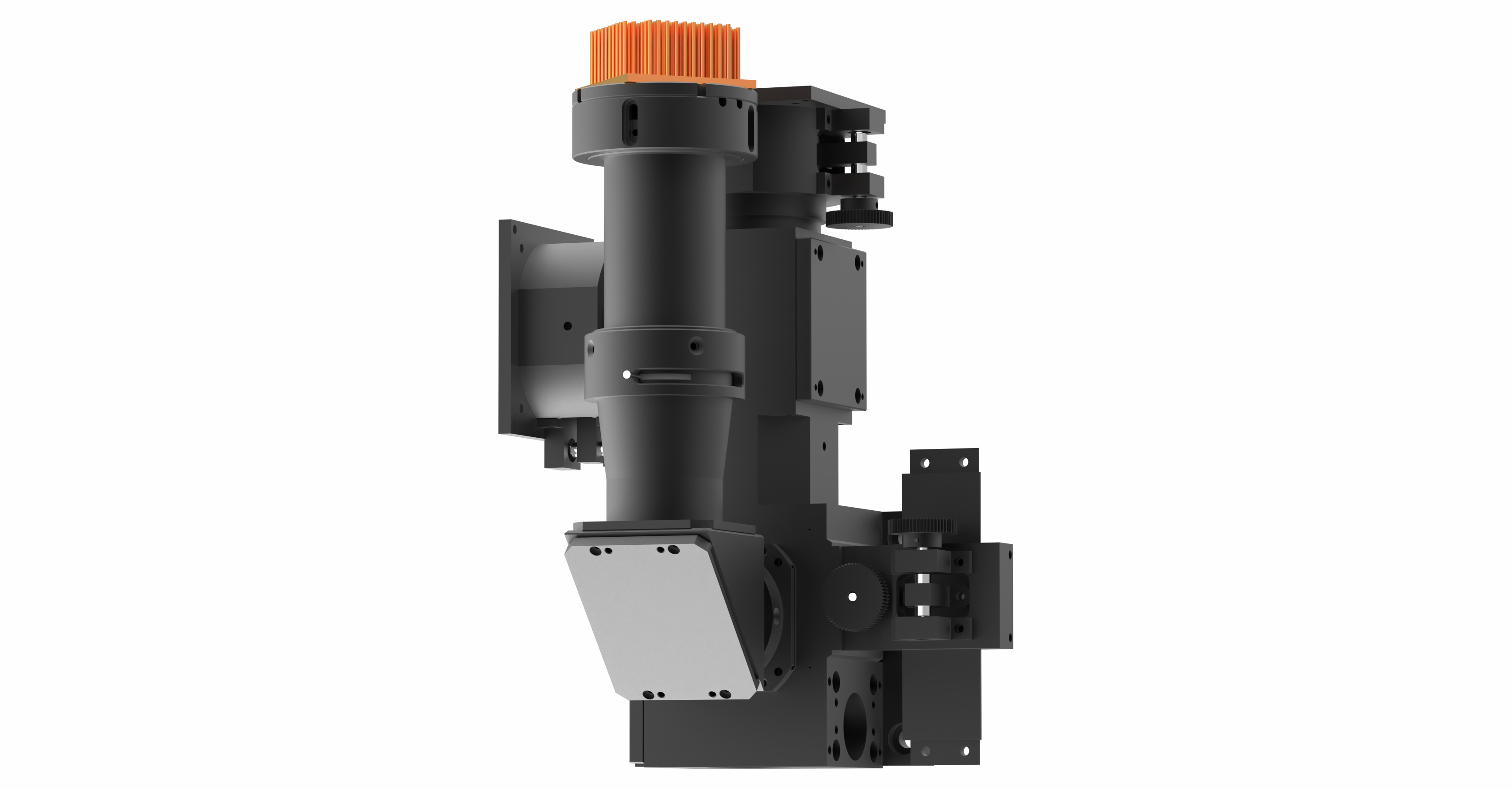
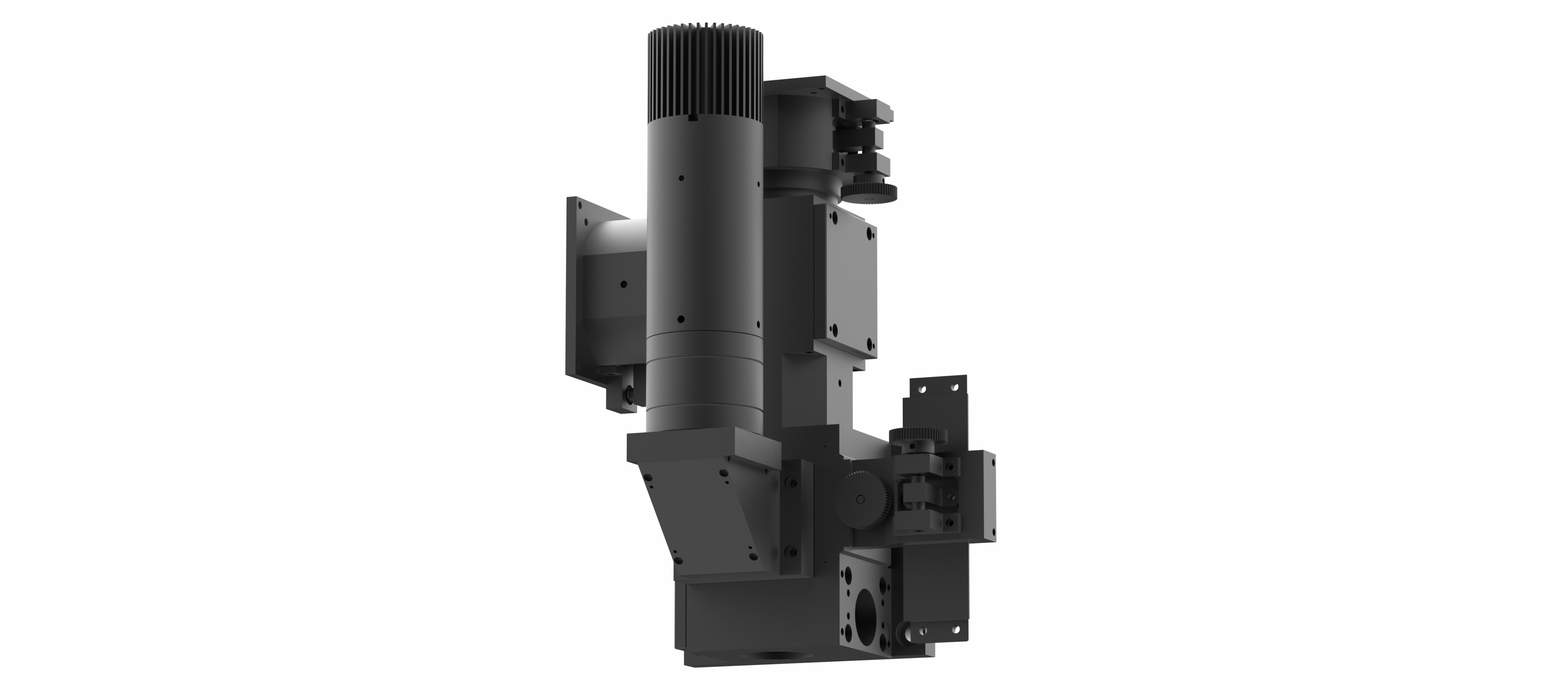
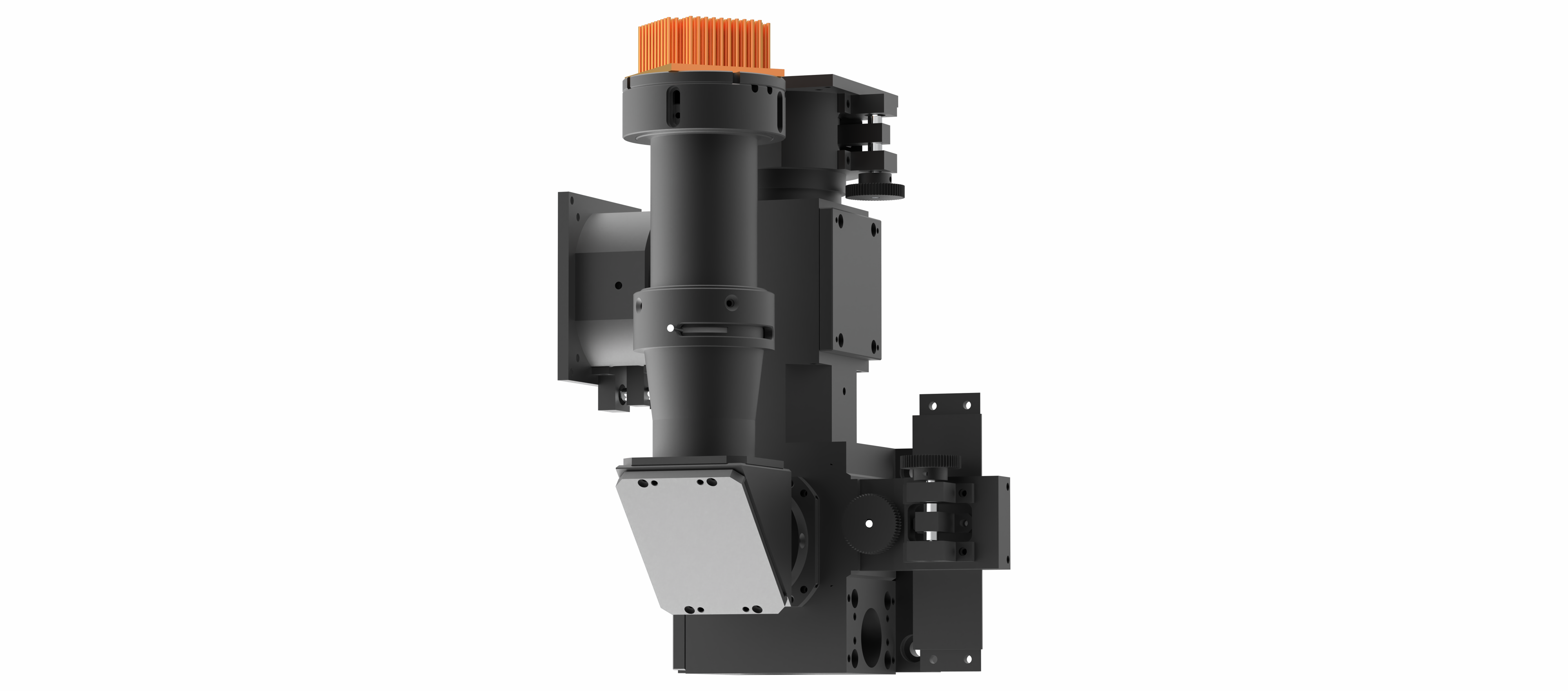
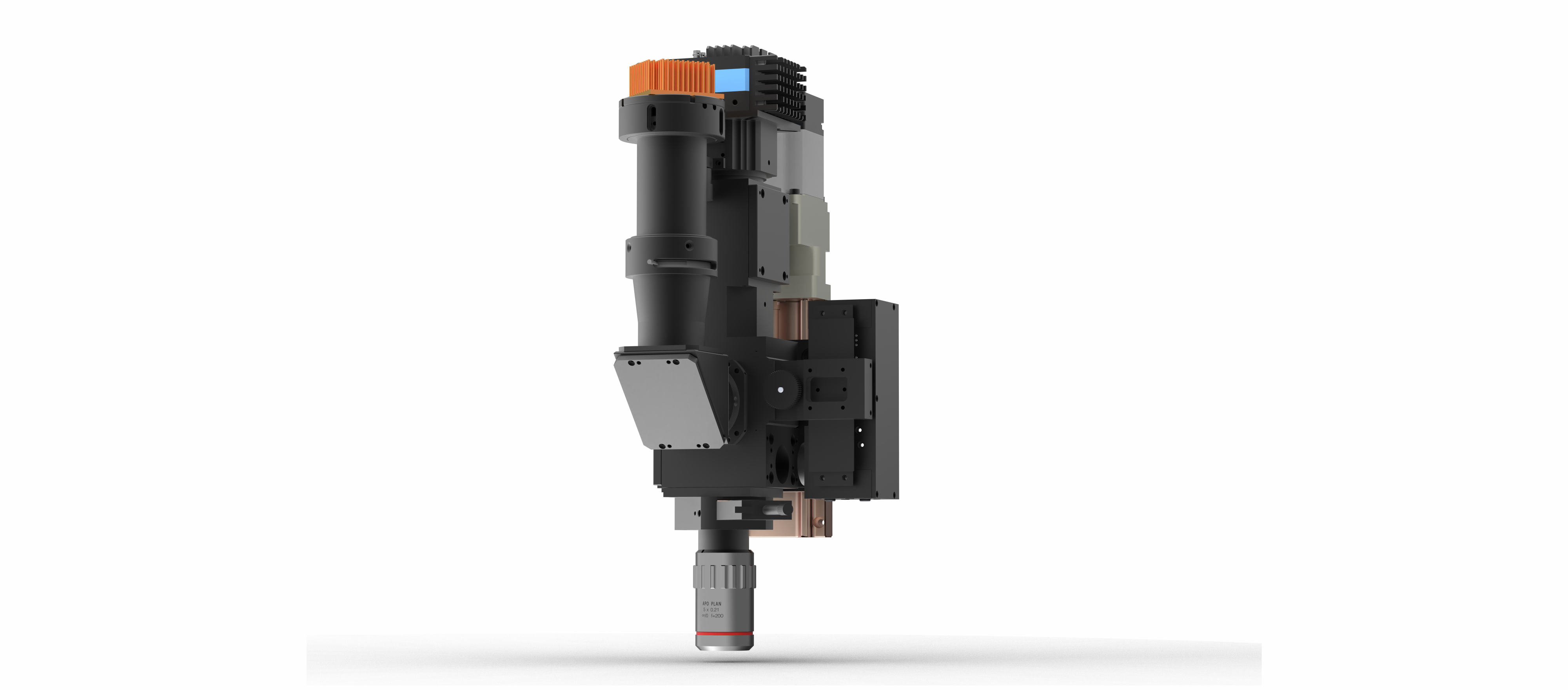
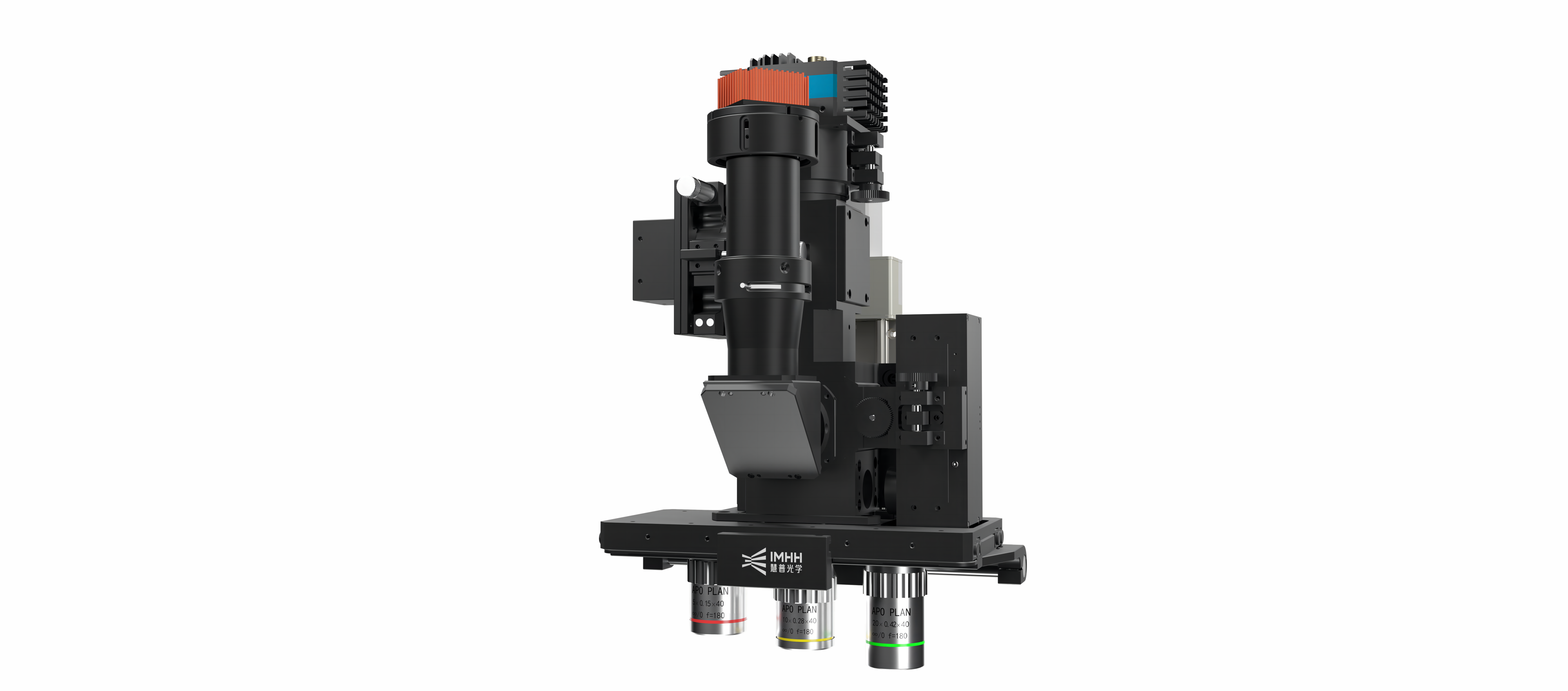
Large field of view lens barrel, maximum support for image side 40mm, perfect for 8K/5um and 65M cameras.
High-resolution lens barrel, the highest object resolution can reach 0.4um.
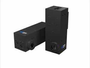
Coaxial laser focusing system can be selected to realize real-time focusing of high-speed motion imaging.
High-speed image focusing system can be selected to solve the problem that laser can't focus accurately under complex background.
Coaxial Kohler lighting, external contact fiber and bright cold light source can support the exposure time of area array camera within 5us.
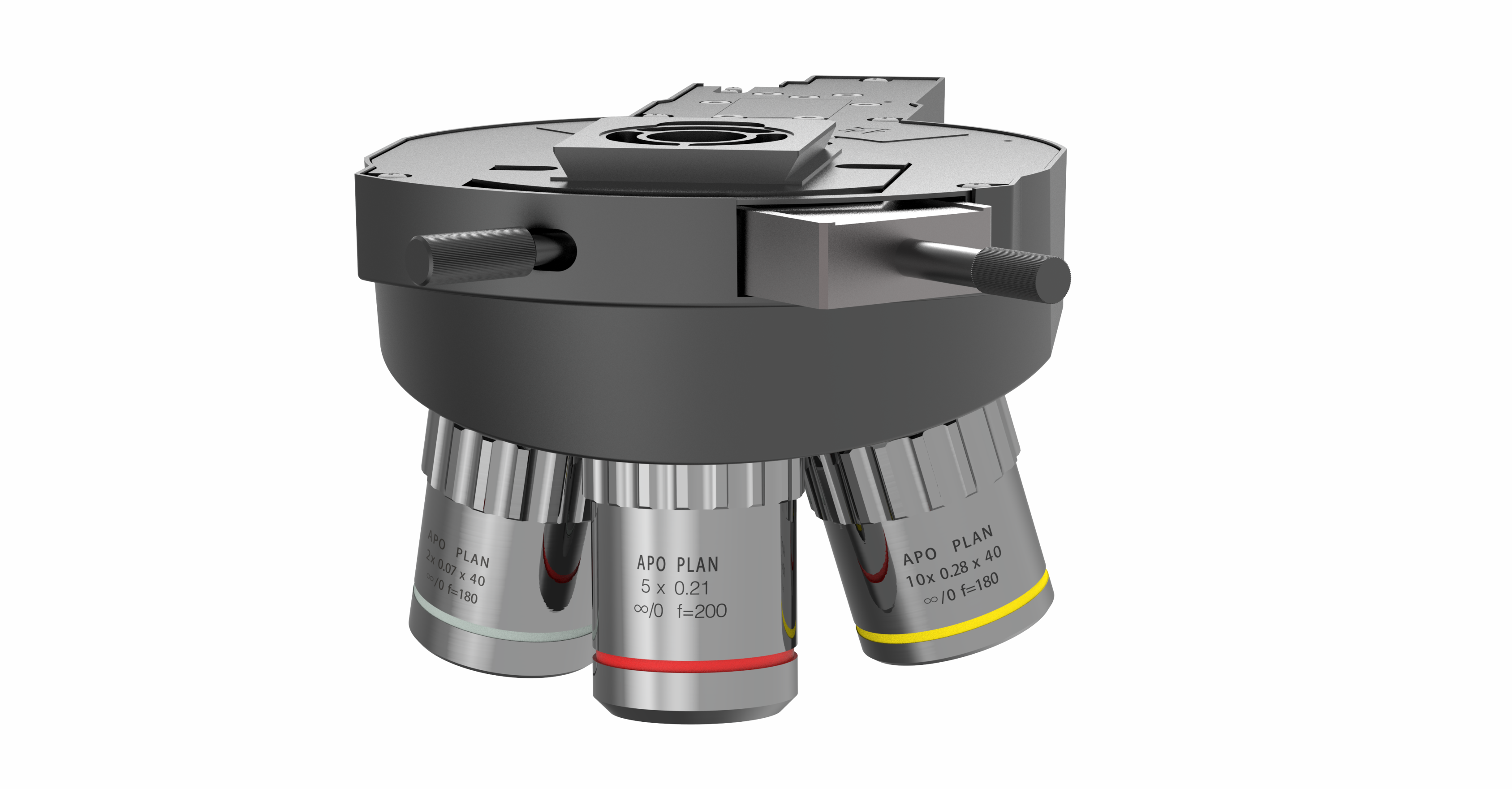
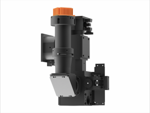
Push-pull high-precision switcher can also support 40mm large field of view of the image.
The dark field illumination angle can be customized to adapt to different application scenarios.
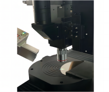
The detection of surface defects (such as scratches, stains, cracks) and internal microstructures (such as circuit layout, transistors) on wafers requires a resolution of micrometers or even sub micrometers. Traditional microscopy systems are difficult to meet the stable focusing requirements under high-speed motion due to issues such as insufficient depth of field and limited field of view.
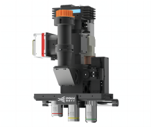
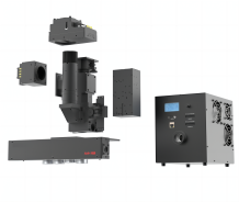
The autofocus microscopy system tracks the height changes of the wafer surface in real time through laser technology and adjusts the focal length of the objective lens to ensure that the image is always clear.
The wafer may be deformed by hundreds of microns in the manufacturing process, while the minimum depth of field of the traditional objective lens may be less than 1 micron, which leads to defocusing during high-speed imaging. Auto-focusing system (such as "Honghu" system) can adjust the Z-axis position in real time through coaxial laser focusing and 5kHz pulse signal, so as to maintain the focusing stability in high-speed movement and greatly improve the detection efficiency.
In addition, the large field of view microscope system is suitable for high-resolution cameras (such as 8K linear camera), which reduces the scanning times and further shortens the detection time.
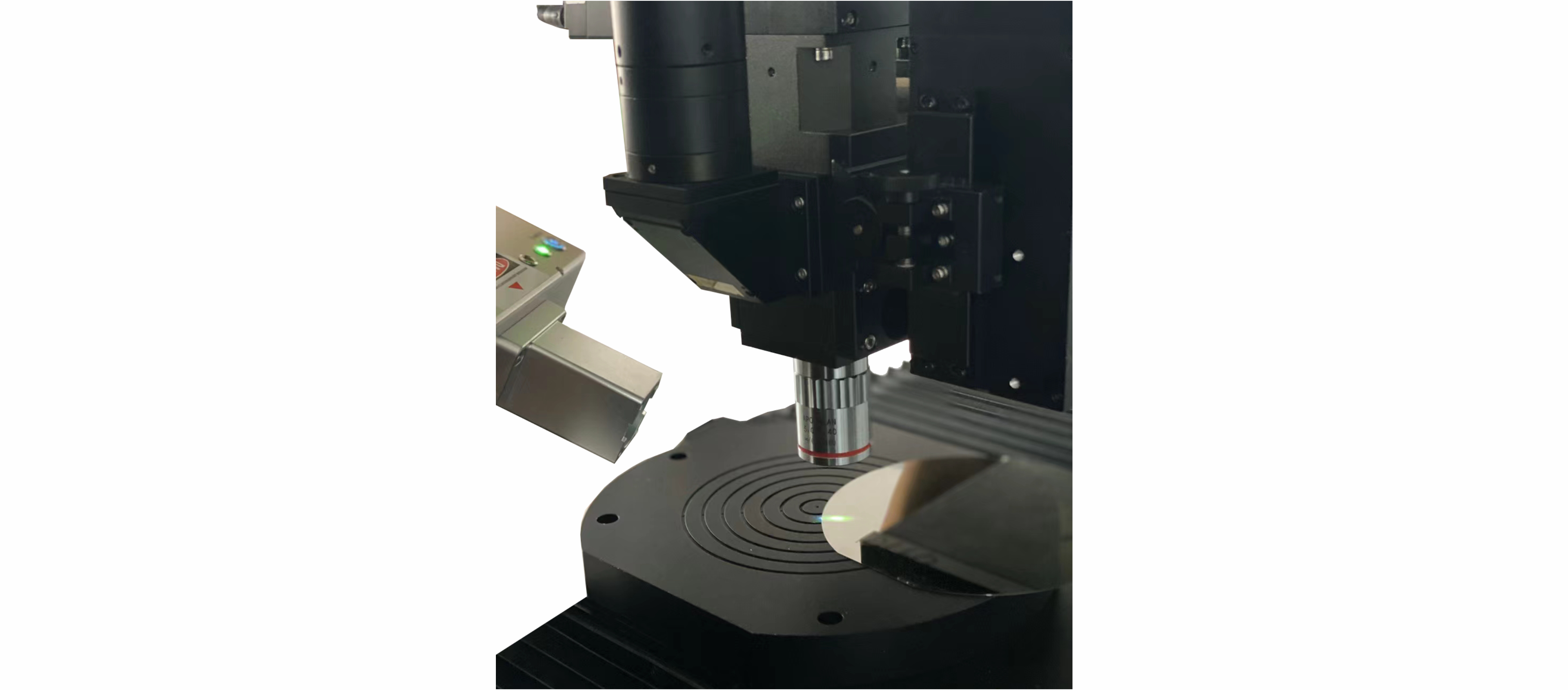
The wafer material is fragile, and traditional contact inspection may introduce damage or pollution. Laser autofocus system completes detection by non-contact way, which avoids the risk brought by physical contact, and is compatible with visible light and short-wave infrared imaging, and adapts to a variety of detection scenarios.
Lithography is a key step in semiconductor manufacturing, and automatic focusing system can monitor the accuracy and consistency of patterns in real time.
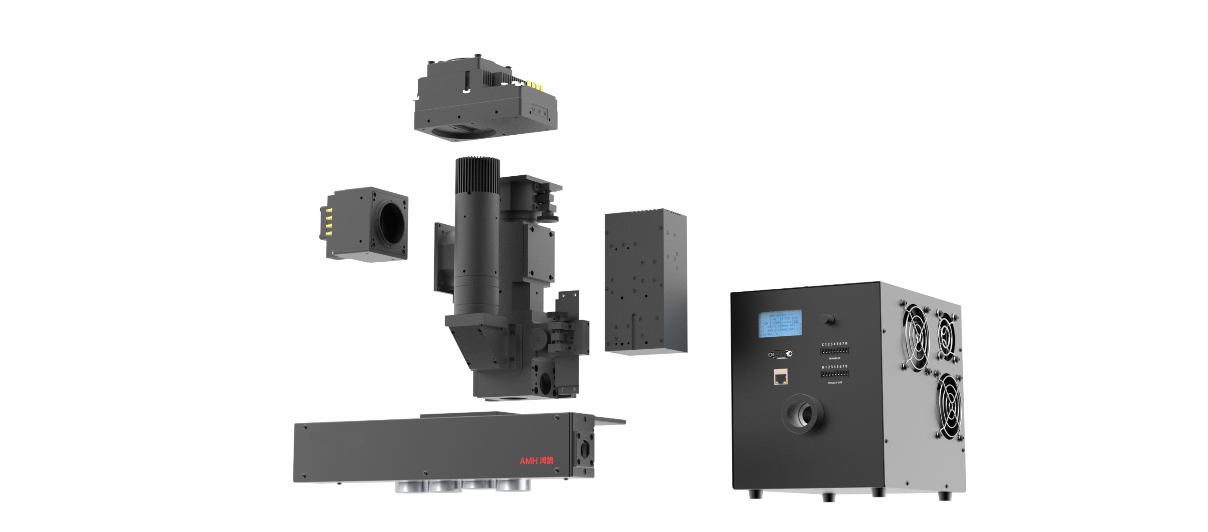
Modern auto-focus systems (e.g., the "Honghu" series) employ modular architecture supporting multi-mode imaging configurations, including visible spectrum, infrared imaging, and polarized light/DIC (Differential Interference Contrast) modes. This plug-and-play modularity enables streamlined prototype assembly tailored to specific application requirements. For instance, microscopic imaging systems with multi-band compatibility (400-1300nm spectral range) can concurrently address both routine wafer inspection and specialized material analysis demands in semiconductor manufacturing processes.
Auto-focusing microscope system has become an indispensable technology for wafer inspection through high-precision tracking, non-contact inspection, high-speed response and multi-scene compatibility. It not only improves the efficiency of defect identification and process stability, but also reduces the production cost and defective rate. It is a key tool for semiconductor manufacturing to move towards intelligence and automation.
Contact: Ms. Liang
Phone: 13922529843
Company email: info@hpoptics.com
human resources: info@hpoptics.com
Dongguan Company: Room 113, Building 3-4, New Base Industrial Park, Xinji Road, Nancheng District, Dongguan City, Guangdong Province
Beijing Company: A301, 3rd Floor, B2 Building, North Territory, Dongsheng Science and Technology Park, Zhongguancun, Haidian District, Beijing
Suzhou Company: Room 415, Jincheng Science and Technology Innovation Park, Louyang Road, Industrial Park, Suzhou City, Jiangsu Province
Plsease input value
Error E-mail format
Plsease input value
Plsease input value